Öffnet in neuem Fenster Opens in a new window Öffnet externe Seite Opens an external site Öffnet externe Seite in neuem Fenster Opens an external site in a new window

Innovation Lab HySPRINT

Generative manufacturing processes for hybrid components (Joint lab with HU Berlin)

Joint lab 4 - enlarged view

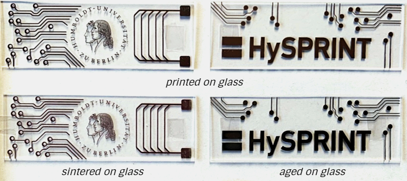
HU and HySPRINT logos inkjet-printed and cured using Cu nanoparticle ink © Prof. Dr. List-Kratochvil, HU

Since August 2018, the HZB group of Dr. Eva Unger (Hybrid Materials Formation and Scaling), who are based in the HySPRINT perovskite lab, and the group of Prof. Dr. Emil List-Kratochvil (Hybrid Devices) from the Integrative Research Institute for the Sciences (IRIS) of Humboldt-Universität zu Berlin (HU Berlin), have cooperated on the long-term project “Generative manufacturing processes for hybrid components” (GenFab).

List-Kratochvil and Unger develop large scale (opto)electronic devices, printed solar cells and components fabricated by printing and solution-based methods from hybrid materials: from transparent conductive electrodes to memory devices, transistors, light-emitting diodes, solar cells and sensor applications.

To enforce the synergy between the research groups, they decided to establish a new jointly used lab space for GenFab based in the new IRIS research building. The joint research place will open in summer/autumn 2020.


Inkjet Printing of Electronics

The use of solution-processable materials for the fabrication of electronic and optoelectronic devices enables the implementation of scalable processing techniques such as printing. As opposed to techniques used to coat entire surface areas, by printing it is possible to directly write arbitrary patterns on a variety of surfaces without the need for masks or structural pre-patterning.

Within our labs of both GEN_FAB and Hybrid Devices, we implement printing processes for a range of material classes, such as conductive inks and polymers. We investigate ink parameters such as viscosity and surface tension and understand surface properties through contact angle measurements. By understanding these properties, we can influence the printing parameters, while through appropriate post-processing, the printed material is then turned into a fully functional material.

Through the use of multiple printheads we are able to produce several inkjet-printed layers within a single machine. Additionally, we use combinatorial approaches through multiple printhead inkjet printing to screen inks and optimize ink compositions.

Finally, we use 3D printing in the form of fused deposition printing and stereolithography to allow us to produce complex custom parts for our scientific setups.

Hybrid Materials Formation and Scaling (HZB)

The Young Investigator Group of Dr. Eva Unger develops scalable deposition methods for fabrication of large scale hybrid and perovskite-based photovoltaic devicesis, using the HySPRINT perovskite lab facilities.

Hybrid Devices (HU)

The group of Prof. Dr. Emil List-Kratochvil performs:

  • coating and inkjet printing using various inks, e.g. metal nanoparticles such as silver and copper;
  • fabrication of the devices up to A4-scale (21 x 30 cm);
  • structural and morphological characterisation of the final components and devices via scanning electron microscopy (SEM), atomic force microscopy (AFM), X-ray photoelectron spectroscopy (XPS)
  • optical and electrical investigations by means of luminance / current / voltage measurements, four-point conductivity (see the photo), external quantum efficiency and others.

    More details on the availabale methods and research progress of the "Hybrid Devices" group can be found here.

Read more: HySPRINT upgraded. Joint lab with Humboldt Universität